
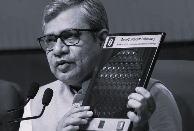
Semicon India Gains Pace as Ashwini Vaishnaw Sets 24-Month Analog IP Target
India’s semiconductor ambitions are shifting from policy vision to on-ground execution, with the Centre intensifying its push on chip design, domestic intellectual property, and ecosystem development. Union Minister for Electronics and IT Ashwini Vaishnaw said India’s semiconductor design programme has reached a significant stage, positioning the country for stronger advances in the global chip industry. He recently interacted with 23 chip design companies selected under the Semicon India Programme’s Design Linked Incentive (DLI) scheme , signalling measurable progress.
According to the minister, what began three years ago as policy groundwork has evolved into working projects and prototypes. Indian startups and design firms are moving beyond concepts and demonstrating practical chip solutions, strengthening investor confidence and easing access to funding. This marks India’s growing presence in the global semiconductor value chain, especially in design and intellectual property creation.
The push is anchored by the India Semiconductor Mission (ISM) , backed by a central outlay of ₹76,000 crore , aimed at building a complete semiconductor ecosystem spanning design, manufacturing, packaging, testing, and research. The DLI scheme supports this by covering up to 50% of eligible design costs and offering sales-linked incentives. Through CDAC , companies also receive access to expensive Electronic Design Automation (EDA) tools free of cost, lowering entry barriers for domestic firms.
Among companies participating in the DLI-backed design ecosystem are Saankhya Labs , known for communication chipsets; Vervesemi Microelectronics , working on advanced analog and mixed-signal ICs; C2i Semiconductors , Linesemi Technology , Nanojoules Semiconductors , and CIMware Technologies , which have received EDA support; and Aryabhata Circuits , engaged in semiconductor circuit design. Their projects span communication SoCs, microprocessor IP cores, surveillance and energy metering chips, and networking solutions reflecting diverse, application-focused semiconductor efforts.
A key focus area is the development of high-speed analog IP (Intellectual Property) such as USB and PCIe . In semiconductor terms, IP refers to pre-designed, reusable circuit blocks used as building components for chips. Analog IPs are vital as they manage real-world electrical signals including power, communication, and data transfer. Vaishnaw has set a target of developing standard IPs within 24 months and advanced analog IP suites within 36 months .
On the manufacturing side, India is adopting a phased approach, prioritizing ATMP/OSAT facilities , display driver chips, sensors, and compound semiconductors. With projects from players such as Micron and the HCL–Foxconn joint venture, India aims to steadily build capacity while advancing toward long-term semiconductor self-reliance.